Most students encounter the word 'nanotechnology' in a single sentence of their textbook. At INACADEMICS, we treat it as a full lesson arc — one that connects Nobel-Prize-winning physics, real laboratory instrumentation, and exam-style calculation practice in a single, coherent session.
Nanotechnology sits at the intersection of three things the IB DP Physics syllabus rewards: conceptual understanding (AO1), quantitative application (AO2), and the Nature of Science (AO3). Yet many students arrive at exams having only memorised that 'the STM was invented in 1981.' That is not enough for a 7.
We Start With the Story, Not the Definition
Every lesson on nanotechnology at INACADEMICS opens with Richard Feynman's 1959 lecture, 'There's Plenty of Room at the Bottom.' We ask students a simple question before showing them anything:
"If you could pick up a single atom and place it exactly where you wanted — what would you build?"
This question does two things simultaneously. It gives students a genuine stake in the concept before we explain the physics. And it mirrors the exact intellectual journey that led Feynman, and later Binnig and Rohrer at IBM Zürich, to develop the scanning tunnelling microscope (STM) in 1981 — an invention that turned the idea of atomic manipulation from philosophy into engineering.
The historical arc matters. IB examiners frequently frame nanotechnology questions around the development of scientific knowledge — exactly the Nature of Science thread that runs through Paper 3. Students who understand why the STM was transformative (not just what it does) answer those questions at a qualitatively different level.
How We Teach the STM — Concept Visualisation Before Equations
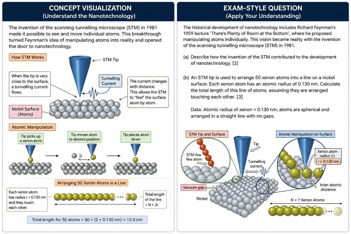
Before any student at INACADEMICS touches a numerical problem, they work through a structured concept visualisation. The diagram below illustrates exactly the resource we use in class.
CONCEPT VISUALISATION: How the STM Works
[Class resource: dual-panel visual — STM mechanism (left) and exam-style question (right)]
The left-hand panel of our class resource shows three physical stages of STM operation that students must be able to explain in their own words:
• Tunnelling current: When an atomically sharp metal tip is brought within a few nanometres of a conducting surface, a quantum tunnelling current flows across the vacuum gap — even though the tip never touches the surface.
• Distance sensitivity: This tunnelling current changes exponentially with tip-to-surface distance. A variation of just 0.1 nm in distance changes the current by roughly one order of magnitude. This extraordinary sensitivity allows the STM to 'feel' individual surface atoms.
• Atomic manipulation: By adjusting the tip-to-surface voltage and current, the STM can pick up a single atom, transport it laterally, and place it at a precise target location on the surface. This three-step sequence — pick up, move, place — is exactly what students need to describe in an exam.
The 1989 IBM experiment in which Eigler and Schweizer used an STM to spell 'IBM' in 35 xenon atoms on a nickel surface is our go-to demonstration example. It is historically real, it is visually striking, and it is quantitatively tractable — making it ideal for the calculation questions that follow.
The Exam-Style Calculation — Worked Through in Class
The right-hand panel of our resource presents the exam-style question directly alongside the concept. This is deliberate. Students see that the diagram they have just analysed conceptually is also the source of the numerical data.
Exam-Style Question (3 marks)
An STM tip is used to arrange 50 xenon atoms into a straight line on a nickel surface. Each xenon atom has an atomic radius of 0.130 nm. The atoms are spherical and arranged touching each other with no gaps. Calculate the total length of this line of atoms.
How We Walk Students Through This — Step by Step
In our small-batch sessions of 4–8 students, we use a structured three-step approach for every calculation in nanotechnology:
Step
What We Ask Students To Do
Why It Matters for IB Marking
1
Identify the geometry
Each atom is a sphere of radius r = 0.130 nm, so its diameter is 2r = 0.260 nm. When touching in a line, the centre-to-centre distance equals one full diameter.
2
Write the formula and substitute
Total length = N × 2r = 50 × (2 × 0.130 nm) = 50 × 0.260 nm. Full working must be shown for mark-scheme compliance.
3
State the answer with correct units and sig figs
Total length = 13.0 nm. Three significant figures matches the data given (0.130 nm). Unit omission costs a mark in IB marking.
The answer — 13.0 nm — is deceptively simple. What distinguishes a 7 student from a 5 student is not the arithmetic. It is the discipline of showing the formula, the substitution, and the correctly unitised answer as three independently identifiable mark points. This is what we train in every session.
The Exam Marking Insight That Changes Student Scores
One of the most impactful things we share with students about nanotechnology calculations is how IB mark schemes actually work. The three marks in a question like this are almost always:
• Mark 1 — correct formula or identification of relevant relationship (L = N × 2r)
• Mark 2 — correct substitution with all values
• Mark 3 — correct final answer with unit
A student who jumps straight to the answer and writes '13 nm' scores only 1 mark out of 3, or possibly 0 if they make an arithmetic error with no recoverable working. A student who shows every step, even if they make a minor arithmetic slip, can score 2 out of 3 through error-carried-forward credit.
INACADEMICS Teaching Rule:
In a 'Calculate' question, you are being marked on your method, not just your answer. Show every step as if the examiner cannot read your mind.
Teaching the Descriptive Part — What 'Describe' Actually Requires
The other sub-question in our resource asks students to describe how the STM contributed to the development of nanotechnology. This is a [2] mark descriptive question. Students consistently underperform here by writing one vague sentence when two distinct, independent mark points are required.
We train students to decompose this into a two-part answer structure:
Common Student Answer (1/2 marks)
INACADEMICS Trained Answer (2/2 marks)
"The STM allowed scientists to see atoms for the first time, which helped develop nanotechnology."
"The STM enabled imaging of individual atoms by detecting changes in tunnelling current with distance [mark 1]. It also allowed manipulation of individual atoms by picking up and precisely repositioning them on a surface [mark 2]."
The difference is structural discipline: the student knows to give two mechanistically distinct statements, not one padded sentence. This is a learnable skill, and it is exactly what our small-batch teaching environment is designed to develop.
The INACADEMICS Approach: Visual–Conceptual–Quantitative
Our nanotechnology sessions are built on a three-stage learning sequence that we apply across all IB DP Physics topics:
1. Visual first — every abstract concept is anchored in a labelled diagram before a single formula appears.
2. Conceptual bridge — students verbalise the physics in their own words, connecting the diagram to the underlying mechanism.
3. Quantitative last — calculations are introduced only after the student can explain what each variable represents physically.
This sequence matters because IB DP Physics Paper 2 and Paper 3 questions almost always combine a conceptual 'Describe' or 'Explain' sub-part with a numerical 'Calculate' sub-part on the same stem. A student who has only practised calculations will freeze on the descriptive question. A student trained in the full arc answers both with confidence.
Why Small Batches Make a Difference:
In a batch of 4–8 students, every learner verbalises their reasoning in every session. There is no hiding behind a larger group. Our certified IB teachers identify and correct conceptual misconceptions in real time — the kind that only surface when a student is asked to explain, not just calculate.
Supplementing Class Work With INACADEMICS
For students who want additional criterion-aligned practice on nanotechnology and other IB DP Physics topics, our platform INACADEMICS (INACADEMICS.COM) hosts a curated library of over 100,000 questions built by IB subject experts.
Every question on INACADEMICS is tagged by topic, sub-topic, command term, and mark allocation — so students practising nanotechnology calculations can filter specifically for 'Calculate' questions at the 3-mark level, or 'Describe' questions requiring two independent mark points. Practice is targeted, not random.
Frequently Asked Questions About Nanotechnology in IB DP Physics
Q: Is nanotechnology a compulsory topic in IB DP Physics?
Nanotechnology appears in the IB DP Physics course as part of the Nature of Science and as a context within core topics including atomic and nuclear physics, and measurement. While specific mark allocations vary by examination session, understanding the STM, atomic manipulation, and nanoscale calculations is regularly examined in Paper 2 and Paper 3.
Q: What level of mathematical skill does nanotechnology require in IB DP Physics?
The calculations are not mathematically complex — they involve multiplication and conversion of units (nm to m, or m to nm). The challenge is conceptual: students must know why the formula L = N × 2r works, not just how to apply it. IB examiners regularly award marks for method, not just correct answers.
Q: How does the STM differ from an electron microscope?
An electron microscope images surfaces by detecting scattered electrons — it is fundamentally a passive observer. The STM detects quantum tunnelling current and can actively manipulate individual atoms. This ability to both image and modify matter at the atomic scale is what makes the STM the foundational tool of nanotechnology.
Q: What is the significance of the 1989 IBM xenon experiment?
Eigler and Schweizer at IBM used an STM to position 35 xenon atoms on a nickel surface to spell 'IBM' — demonstrating for the first time that individual atoms could be placed with deliberate precision. This is the direct scientific ancestor of the calculation type above (50 atoms, 13.0 nm total length) and is the standard narrative context in IB DP Physics examination questions on nanotechnology.